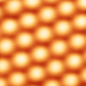
- Image via Wikipedia
Manufacturing With Every Atom in Its Proper Place May Be Coming Soon
The long-held dream of creating atomically precise three-dimensional structures in a manufacturing environment is approaching reality, according to the top scientist at a company making tools aimed at that ambitious goal.
John Randall, Vice President of Zyvex Labs in Richardson, Tex., says his researchers have demonstrated a process that uses a scanning tunneling microscope tip to remove protective surface hydrogen atoms from silicon one at a time and then adds single atomic layers of silicon only to those meticulously cleared areas. Randall describes the achievement at the AVS 57th International Symposium & Exhibition, which takes place this week in the Albuquerque Convention Center in New Mexico.
To date, Zyvex Labs researchers have demonstrated removal of 50 hydrogen atoms per second. But with experience and innovation, Randall predicts large improvements in the speed of this limiting factor.
“There are many paths to scale-up, including parallelism,” he says. “A thousand-fold increase in speed will be fairly easy to achieve.”
Within seven years, Randall expects that Zyvex Labs will be selling initial production tools that can remove more than a million hydrogen atoms a second using 10 parallel tips at a cost of about $2,000 per cubic micrometer of added silicon (48 billion atoms).
Applications that would benefit most from having tiny atomically precise structures include nanopore membranes, qubit structures for quantum computers and nanometrology standards. Larger-scale applications, such as nanoimprint templates, would need still further cost-performance improvements to become economically viable.
The Latest Streaming News: Atomic-Level Manufacturing updated minute-by-minute


