


Billions of objects ranging from smartphones and watches to buildings, machine parts and medical devices have become wireless sensors of their environments, expanding a network called the “Internet of Things.”
As society moves toward connecting all objects to the internet – even furniture and office supplies – the technology that enables these objects to communicate and sense each other will need to scale up.
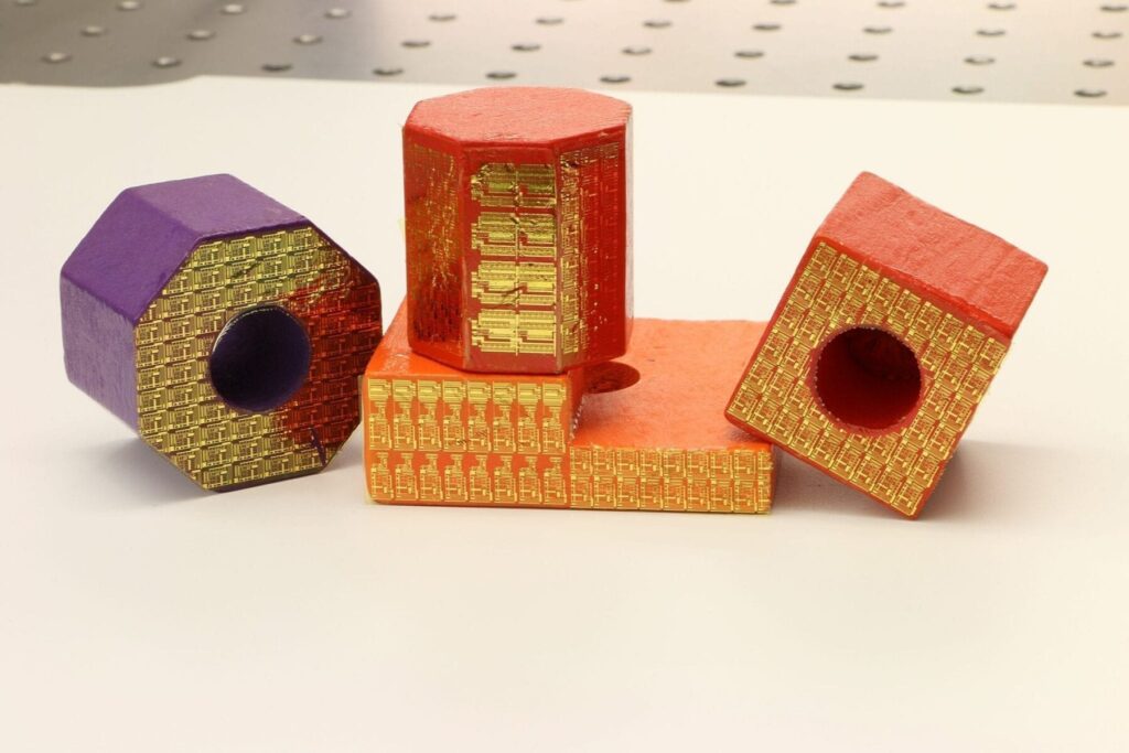
Researchers at Purdue University and the University of Virginia have developed a new fabrication method that makes tiny, thin-film electronic circuits peelable from a surface. The technique not only eliminates several manufacturing steps and the associated costs, but also allows any object to sense its environment or be controlled through the application of a high-tech sticker.
Eventually, these stickers could also facilitate wireless communication. The researchers demonstrate capabilities on various objects in a paper recently published in the Proceedings of the National Academy of Sciences.
“We could customize a sensor, stick it onto a drone, and send the drone to dangerous areas to detect gas leaks, for example,” said Chi Hwan Lee, Purdue assistant professor of biomedical engineering and mechanical engineering.
Most of today’s electronic circuits are individually built on their own silicon “wafer,” a flat and rigid substrate. The silicon wafer can then withstand the high temperatures and chemical etching that are used to remove the circuits from the wafer.
But high temperatures and etching damage the silicon wafer, forcing the manufacturing process to accommodate an entirely new wafer each time.
Lee’s new fabrication technique, called “transfer printing,” cuts down manufacturing costs by using a single wafer to build a nearly infinite number of thin films holding electronic circuits. Instead of high temperatures and chemicals, the film can peel off at room temperature with the energy-saving help of simply water.
“It’s like the red paint on San Francisco’s Golden Gate Bridge – paint peels because the environment is very wet,” Lee said. “So in our case, submerging the wafer and completed circuit in water significantly reduces the mechanical peeling stress and is environmentally friendly.”
A ductile metal layer, such as nickel, inserted between the electronic film and the silicon wafer, makes the peeling possible in water. These thin-film electronics can then be trimmed and pasted onto any surface, granting that object electronic features.
Putting one of the stickers on a flower pot, for example, made that flower pot capable of sensing temperature changes that could affect the plant’s growth.
Lee’s lab also demonstrated that the components of electronic integrated circuits work just as well before and after they were made into a thin film peeled from a silicon wafer. The researchers used one film to turn on and off an LED light display.
“We’ve optimized this process so that we can delaminate electronic films from wafers in a defect-free manner,” Lee said.
Learn more: Electronic stickers to streamline large-scale ‘Internet of Things’

The Latest on: Peelable thin-film electronic circuits
[google_news title=”” keyword=”peelable thin-film electronic circuits” num_posts=”10″ blurb_length=”0″ show_thumb=”left”]
via Google News
The Latest on: Peelable thin-film electronic circuits
- Research team develops new thin film deposition process for tin selenide-based materialson May 9, 2024 at 6:45 am
This advanced process allowed for the uniform deposition of thin films at a low temperature of approximately 200°C, regardless of the substrate used, showcasing its potential for various electronic ...
- Researchers identify cause of electron-hole separation in thin-film solar cells to increase solar cell efficiencyon May 8, 2024 at 6:38 am
A team of researchers have collaborated to characterize electron-hole separation in the light-absorbing layer of kesterite thin-film solar cells. This study is expected to improve the efficiency of ...
- Opening up the potential of thin-film electronics for flexible chip designon April 24, 2024 at 8:04 am
New research by KU Leuven and imec shows that this ‘foundry’ model can also be applied to the field of flexible, thin-film electronics. Adopting this approach would give innovation in the ...
- Opening up the potential of thin-film electronics for flexible chip designon April 23, 2024 at 5:00 pm
The mass production of conventional silicon chips relies on a successful business model with large 'semiconductor fabrication plants' or 'foundries'. New research by shows that this 'foundry' model ...
- Digital Integrated Circuitson April 17, 2024 at 5:00 pm
New Yorker Electronics has signed a franchised distribution agreement with Geyer Electronic, a manufacturer of quart crystals, oscillators and resonators. “Founded in 1964 in Munich as a retail store ...
- New colorful plastic films for versatile sensors and electronic displayson April 15, 2024 at 9:04 am
Innovative electronics is one of the many applications ... "We're excited by the versatility of our thin films," says Youhei Takeda, senior author. "We can use the bipolarity of the phenazaboride ...
- Thin oil films enable stable oil and water mixtures sans surfactanton April 10, 2024 at 5:00 pm
Thin oil films absorbed onto the surface of water droplets lead to anomalously stable, surfactant-free oil and water mixtures, according to a new study. The findings demonstrate a mechanism for ...
- What is Electrical Engineering?on February 29, 2024 at 5:12 pm
Today, we have access to electronic surveillance, medical imaging, computers, and the internet. Electrical engineers work on a wide range of tasks including designing circuits for smartphones and ...
- Electronic Thin-Film Reliabilityon June 24, 2023 at 9:06 pm
Thin films are widely used in the electronic device industry. As the trend for miniaturization of electronic devices moves into the nanoscale domain, the reliability of thin films becomes an ...
via Bing News

