


He is developing next-generation, nanoscale transistors for integrated electronics
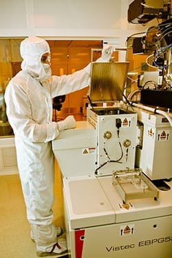
The new electron beam writer housed in the Nano3 cleanroom facility at the Qualcomm Institute is important for electrical engineering professor Shadi Dayeh’s two major areas of research. He is developing next-generation, nanoscale transistors for integrated electronics; and he is developing neural probes that have the capacity to extract electrical signals from individual brain cells and transmit the information to a prosthetic device or computer. Achieving this level of signal extraction or manipulation requires tiny sensors spaced very closely together for the highest resolution and signal acquisition. Enter the new electron beam writer.
Electron beam (e-beam) lithography enables researchers to write very small patterns on large substrates with a high level of precision. It is a widely used tool in information technology and life science. Applications range from writing patterns on silicon and compound semiconductor chips for electronic device and materials research to genome sequencing platforms. But the ability to write patterns on the scale afforded by the Nano3 facility—with its minimum feature size of less than 8 nanometers on wafers with diameters that can be as large as 8 inches—is unique in Southern California. Before the facility opened earlier this year, the closest comparable e-beam writer was in Los Angeles. In an e-beam writer, unique patterns are “written” on a silicon wafer coated with a polymer resist layer that is sensitive to electron irradiation. The machine directs a narrowly focused electron beam onto the surface marking the pattern, making parts of the resist coating insoluble and others soluble. The soluble area is later washed away, revealing the pattern which can have sub-10 nanometer feature dimensions.
Bioengineering professor Todd Coleman will use the new e-beam writer as one essential step in the building of his epidermal, or tattoo, electronic devices. The devices are designed to acquire brain signals for a variety of medical applications, from monitoring infants for seizures in neonatal intensive care to studying the cognitive impairment associated with Alzheimer’s disease or dementia, and soldiers struggling with post-traumatic stress syndrome.
Electrical engineering Ph.D. candidate Andrew Grieco is using the machine to develop a new type of optical waveguide that promises to improve efficiency and reduce power consumption. Grieco works in the laboratory of Shaya Fainman, professor and chair, Department of Electrical and Computer Engineering. Developing on-chip optical networking devices such as waveguides, switches and amplifiers is a critical step in the development of optical chips. Although information systems rely primarily on fiber-optic networks to connect and share data around the world, the underlying computer technology is still based on electronic chips, causing data traffic jams.

The Latest Bing News on:
Electron Beam Writer
- Transmitting quantum information using electron spinon May 12, 2024 at 1:55 pm
In the realm of quantum information science, researchers are constantly exploring new ways to extend the boundaries of information storage.
- E-Beam provider NextBeam Expands Team to Drive Customer Focus and Support Growthon May 10, 2024 at 9:29 am
Lindsey’s onboarding supports NextBeam’s growing momentum. In 2023, NextBeam achieved remarkable milestones, including the irradiation of over 5.7 million pounds of customer products and maintaining ...
- Dogged Dark Matter Hunters Find New Hiding Places to Checkon May 7, 2024 at 7:38 am
Perhaps dark matter is made of an entirely different kind of particle than the ones physicists have been searching for. New experiments are springing up to look for these ultra-lightweight phantoms.
- Two facilities team up for structural biology advances with X-ray free-electron lasers and exascale computingon May 6, 2024 at 7:42 am
Plans to unite the capabilities of two cutting-edge technological facilities promise to usher in a new era of dynamic structural biology. Through DOE's Integrated Research Infrastructure, or IRI, ...
- MAPPER and TSMC Take Next Step in Exploring Multiple E-beam Lithography for IC Manufacturing at 22 nanometer node and Beyondon April 28, 2024 at 5:00 pm
Multiple e-beam maskless lithography uses over 10,000 electron beams working in parallel to directly write circuit patterns on a wafer, eliminating the need for the costly photomasks used in current ...
- Rocket Lab gearing up to refly Electron booster for 1st timeon April 17, 2024 at 5:00 pm
"This is the exciting final piece of the puzzle before Electron goes reusable." Rocket Lab is taking a big step toward its first-ever rocket reflight. On Jan. 31, one of the company's Electron ...
- Development of Electron Beam and X Ray Applications for Food Irradiationon December 18, 2023 at 12:25 am
including high energy (MeV) and low energy (keV) electron beam and X ray irradiation. Comparative studies of gamma, electron beam and X ray irradiation for food and phytosanitary uses are also ...
- Introduction to Scanning Electron Microscopy (SEM)on June 16, 2023 at 11:43 am
Technological innovations such as Field Emission SEM (FESEM), which uses a field emission gun to provide a smaller and more focused electron beam, and Environmental SEM (ESEM), which allows for the ...
- The Different Types of Lithography in Nanotechnologyon June 16, 2023 at 11:43 am
On the other hand, Electron Beam, Focused Ion Beam, and Dip Pen Nanolithography are slower, serial processes. They require the beam or tip to be scanned across the surface to write each feature, ...
- Vistec SB254: High Performance Electron-Beam Lithographyon December 22, 2022 at 11:24 am
Based on the Variable Shaped Beam (VSB) principle, these tools are utilized in a wide range of existing and emerging semiconductor and nanotechnology applications including silicon direct write, ...
The Latest Google Headlines on:
Electron Beam Writer
[google_news title=”” keyword=”Electron Beam Writer” num_posts=”10″ blurb_length=”0″ show_thumb=”left”]
The Latest Bing News on:
Nanoscale transistors
- ‘They want this, all of it’: The global arms race you can’t see – and China wants the edgeon May 12, 2024 at 4:20 pm
Microchips are key to powering the world. What will it take to win in this vital (and secretive) multi-billion-dollar world?
- The second quantum computing revolutionon May 10, 2024 at 12:45 pm
Madison, students regularly trap single electrons inside silicon chips. They know where the electrons are. They know when they move. And they can monitor that motion in ...
- Single-Electron Transistors: The Ultimate in Miniaturization and Precisionon May 2, 2024 at 9:01 pm
What is a Single-Electron Transistor? A single-electron transistor (SET) is a nanoscale electronic device that allows the precise control of individual electrons. Unlike conventional transistors that ...
- New memory transistor integrates photocrosslinker into molecular switches to adjust its threshold voltageon May 2, 2024 at 9:22 am
A research team has developed a memory transistor capable of adjusting its threshold voltage. This innovation combines two molecules that form a stable bond with a polymeric semiconductor, situated at ...
- Quantum electronics: Charge travels like light in bilayer grapheneon April 16, 2024 at 3:45 pm
energy-efficient transistors – like the light switch in your house but at a nanoscale. The Massachusetts Institute of Technology (MIT), USA, and the National Institute for Materials Science ...
- Quantum electronics: Charge travels like light in bilayer grapheneon April 15, 2024 at 5:00 pm
energy-efficient transistors -- like the light switch in your house but at a nanoscale. An international research team led by the University of Göttingen has demonstrated experimentally that ...
- Single-Molecule Transistor Using Quantum Interferenceon April 15, 2024 at 5:00 pm
This affects the performance of nanoscale transistors, with direct source–drain tunnelling degrading switching ratios and subthreshold swings, and ultimately limiting operating frequency due to ...
- Nanofluidic Transistors: Controlling Fluids at the Nanoscaleon March 14, 2024 at 3:50 am
Nanofluidic transistors, also known as nanofluidic systems or nanofluidic devices, are innovative tools that control the flow of fluids, such as water or ions, through nanoscale channels using ...
- Selective operation of enhancement and depletion modes of nanoscale field-effect transistorson March 6, 2024 at 1:52 pm
More information: Abhay A. Sagade, Selective Operation of Enhancement and Depletion Modes of Nanoscale Field-Effect Transistors, ACS Applied Electronic Materials (2024). DOI: 10.1021/acsaelm.3c01825 ...
- Materials Science and Engineering Summer Instituteon October 5, 2018 at 6:07 am
From the ever-shrinking microchip containing billions of nanoscale transistors to advances in drug delivery for cancer therapy, materials scientists and engineers manipulate atomic structures to ...
The Latest Google Headlines on:
Nanoscale transistors
[google_news title=”” keyword=”nanoscale transistors” num_posts=”10″ blurb_length=”0″ show_thumb=”left”]

