


Could be applied to solar cells, ultracapacitors for energy storage, or advanced transistors for energy efficient electronics, among many other applications
Researchers at Penn State’s Center for 2-Dimensional and Layered Materials and the University of Texas at Dallas have shown the ability to grow high quality, single-layer materials one on top of the other using chemical vapor deposition. This highly scalable technique, often used in the semiconductor industry, can produce new materials with unique properties that could be applied to solar cells, ultracapacitors for energy storage, or advanced transistors for energy efficient electronics, among many other applications.
“People have been trying to stack these layered materials using the scotch tape method (an exfoliation method developed by Nobel laureates Novoselov and Geim to produce graphene), but that leaves residue on the layers and is not scalable,” explains Joshua Robinson of Penn State, corresponding author on a recent article published online in ACS Nano. Other groups have utilized the chemical vapor deposition method to grow layered materials on a copper substrate, but this method requires some sophisticated techniques to transfer the layered material to a more functional substrate without causing tears or contamination.
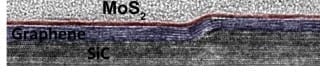
Robinson and his colleagues employed a more direct method, using chemical vapor deposition to grow a layer of quasi-free-standing epitaxial graphene (QFEG) on a silicon carbide substrate, followed by a layer of molybdenum disulfide (MoS2), a metal dichalcogenide compound widely used as a lubricant. In order to test the quality of the MoS2 on graphene, the researchers used the material to build a photodetector device to measure the layered material’s efficiency at converting photons to electrons. They found that the response of the MoS2/QFEG material was 100 times higher than MoS2 alone.
For devices, the QFEG method, which introduces a layer of hydrogen atoms between the substrate and the graphene and thereby decouples the graphene layer from the underlying silicon carbide, proved to be a better choice than the more standard as-grown graphene. Robinson says, “In general QFEG is more interesting, and from a device point of view, it’s critical.”
To see if quasi-free-standing graphene was a suitable template for the growth of other artificially stacked atomic layers, the team synthesized two other van der Waals solids: tungsten diselenide, and hexagonal boron nitride. (van der Waals solids have strong in-plane bonding but weak interlayer bonding.) They determined that epitaxial graphene was “an excellent candidate for building large-area vdW solids that will have extraordinary properties and performances.”
Industry has already shown strong interest in 2D layered materials for RF applications, low-power and low-cost semiconductors, and for displays on flexible substrates. “This is the first step,” Robinson says. “To truly control properties we will need to look at a variety of these systems that should turn out to have entirely new properties when stacked together.”

The Latest on: 2D layered materials
[google_news title=”” keyword=”2D layered materials” num_posts=”10″ blurb_length=”0″ show_thumb=”left”]
via Google News
The Latest on: 2D layered materials
- Beyond Binary: 2D Magnetic Devices Enable Brain-Like Probabilistic Computerson May 10, 2024 at 8:05 pm
University of Wyoming researchers have developed a new method to control magnetic states in 2D materials, promising revolutionary advancements in computing technology and energy efficiency. Imagine a ...
- 2D all-organic perovskites: potential use in 2D electronicson May 9, 2024 at 12:09 pm
Perovskites are among the most researched topics in materials science. Recently, a research team has solved an age-old challenge to synthesize all-organic two-dimensional perovskites, extending the ...
- PolyU researchers create 2D all-organic perovskites and demonstrate potential use in 2D electronicson May 9, 2024 at 7:04 am
Prof. Loh Kian Ping, Chair Professor of Materials Physics and Chemistry and Global STEM Professor of the Department of Applied Physics of PolyU, led a team in the successful synthesis and device ...
- Researchers create 2D all-organic perovskites and demonstrate potential use in 2D electronicson May 8, 2024 at 5:00 pm
This research was published in the journal Science ("Molecularly thin, two-dimensional all-organic perovskites"). Perovskites are named after their structural resemblance to the mineral calcium ...
- Researchers 'unzip' 2D materials with laserson May 8, 2024 at 7:00 am
Researchers used commercially available tabletop lasers to create tiny, atomically sharp nanostructures in samples of a layered 2D material called hexagonal Boron Nitride (hBN). The new ...
- Researchers 'unzip' 2D materials with laserson May 7, 2024 at 8:42 am
In a new paper published on May 1 in the journal Science Advances, researchers at Columbia Engineering used commercially available tabletop lasers to create tiny, atomically sharp nanostructures, or ...
- Columbia researchers “unzip” 2D materials with laserson May 6, 2024 at 4:59 pm
In a new paper in the journal Science Advances, researchers used commercially available tabletop lasers to create tiny, atomically sharp nanostructures in samples of a layered 2D material called ...
- Researchers create 2D all-organic perovskites, demonstrate potential use in 2D electronicson May 6, 2024 at 6:49 am
Perovskites are among the most researched topics in materials science. Recently, a research team from The Hong Kong Polytechnic University (PolyU) has solved an age-old challenge to synthesize ...
- Researchers unlock potential of 2D magnetic devices for future computingon May 1, 2024 at 12:06 pm
Imagine a future where computers can learn and make decisions in ways that mimic human thinking, but at a speed and efficiency that are orders of magnitude greater than the current capability of ...
- Exploiting disorder to harvest heat energy: The potentialities of 2D magnets for thermoelectric applicationson April 30, 2024 at 9:20 am
Thermoelectric systems are a green and sustainable way to harvest energy from any form of heat that otherwise would be wasted. At the core of this energy conversion process is the so-called Seebeck ...
via Bing News

